Professional circuit board manufacturing high tech enterprise
Make high quality high precision printed circuit board

|
24-hour national unified Consulting Hotline |
Professional circuit board manufacturing high tech enterprise
Make high quality high precision printed circuit board
|
24-hour national unified Consulting Hotline |

Phone: +86-752-3198333
Email: sales@xcpcb.net
Website: en.xcpcb.net
Address: South of Lianfa Avenue, Yongqiao Industrial Park, Zhongkai High-tech Zone, Huizhou, Guangdong Province
The production process of PCB is relatively complicated. It involves a wide range of processes, ranging simple mechanical processing to complex mechanical processing, common chemical reactions photochemical electrochemical thermochemical processes, computer-aided design of CAM other knowledge. . in the production process, there are many process problems new problems will be encountered time to time. Some problems disappear without finding out the cause. Because the production process is a discontinuous pipeline form, any problem in any link will cause the entire line to stop production. As a result of a large number of scraps, if printed circuit boards are scrapped, they cannot be recycled reused, process engineers have a greater pressure on work, so many engineers have left the industry transferred to printed circuit board equipment material vendors to do sales technical services.

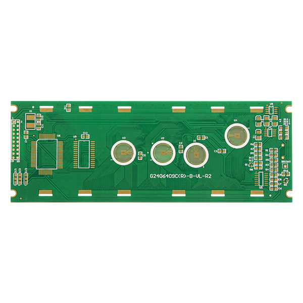
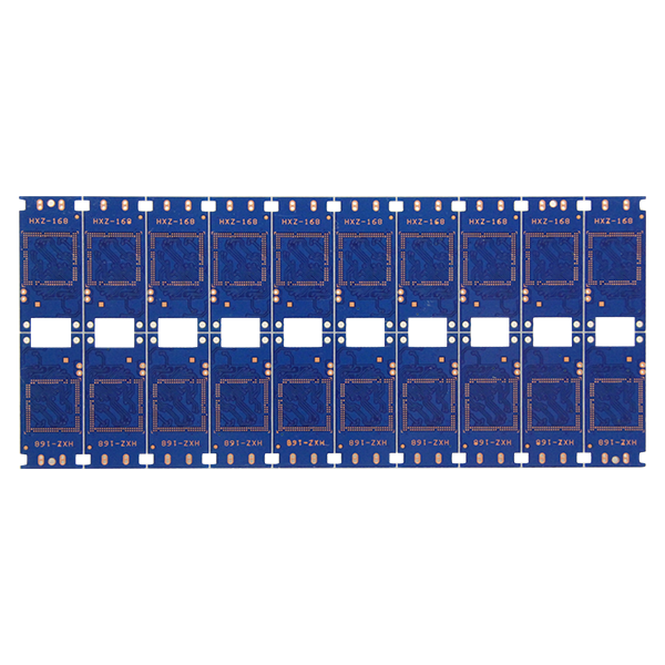
The substrate of the board itself is made of insulating heat-resistant materials that are easy to bend. The fine circuit material that can be seen on the surface is copper foil. After being etched away, the remaining part becomes small mesh-like lines. These lines are called conductor patterns wiring, are used to provide circuit connections for parts on the PCB.
In order to fix the parts on the PCB, we solder their pins directly to the wiring. On the most basic PCB (single panel), the parts are concentrated on one side the wires are concentrated on the other side. You need to make holes in the board so that the pins can pass through the board to the other side, so the pins of the parts are soldered to the other side. Because of this, the front back sides of the PCB are called the component side component side, respectively. Solder Side.
If there are some parts on the PCB that need to be removed replaced after the production is completed, the socket will be used when the part is installed. Since the socket is directly soldered to the board, the parts can be disassembled arbitrarily .
If you want to connect two PCBs to each other, we usually use the edge connector commonly known as "golden finger". The golden finger contains many exposed copper pads, which are actually part of the PCB wiring. When connecting, we usually insert the golden finger on one PCB into the appropriate slot on the other PCB (commonly called the expansion slot Slot). In a computer, such as a graphics card, sound card other similar interface card Are connected to the motherboard by cheat fingers.
The green brown color on the PCB is the color of the solder mask. This layer is an insulating protective layer that can protect the copper wire prevent the parts being soldered to the incorrect place. In addition to the solder mask A silk screen is printed on it. Usually text symbols (mostly white) are printed on it to indicate the position of each part on the board. The silk screen is also called Icon side (legend).
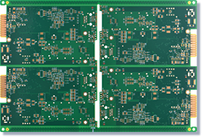
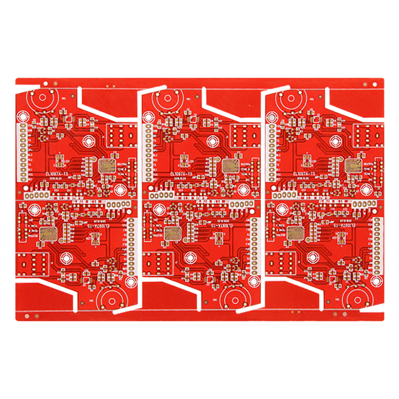
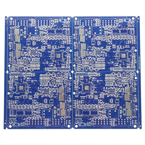
The printed circuit board etches a complex copper wire between parts after careful planning, etches it on a board to provide the main support for electronic components during installation interconnection. It is indispensable for all electronic products. Basic parts.
The printed circuit board is a flat plate made of non-conductive material. The flat plate is usually designed with pre-drilled holes to install chips other electronic components. The holes of the component help to electronically connect the pre-defined metal paths printed on the board, pass the pins of the electronic component through the PCB, then adhere to the PCB with a conductive metal electrode to form a circuit.
Relevant webpage materials related resources on this site are sourced the Internet. If there is any infringement, please inform us quickly. We will delete it within 24 hours! Circuit board manufacturer
Telephone:+86-752-3198333
mailbox:sales@xcpcb.net
address:South of Lianfa Avenue, Tongqiao Industrial Park, Zhongkai high tech Zone, Huizhou City, Guangdong Province