Professional circuit board manufacturing high tech enterprise
Make high quality high precision printed circuit board

|
24-hour national unified Consulting Hotline |
Professional circuit board manufacturing high tech enterprise
Make high quality high precision printed circuit board
|
24-hour national unified Consulting Hotline |

Phone: +86-752-3198333
Email: sales@xcpcb.net
Website: en.xcpcb.net
Address: South of Lianfa Avenue, Yongqiao Industrial Park, Zhongkai High-tech Zone, Huizhou, Guangdong Province
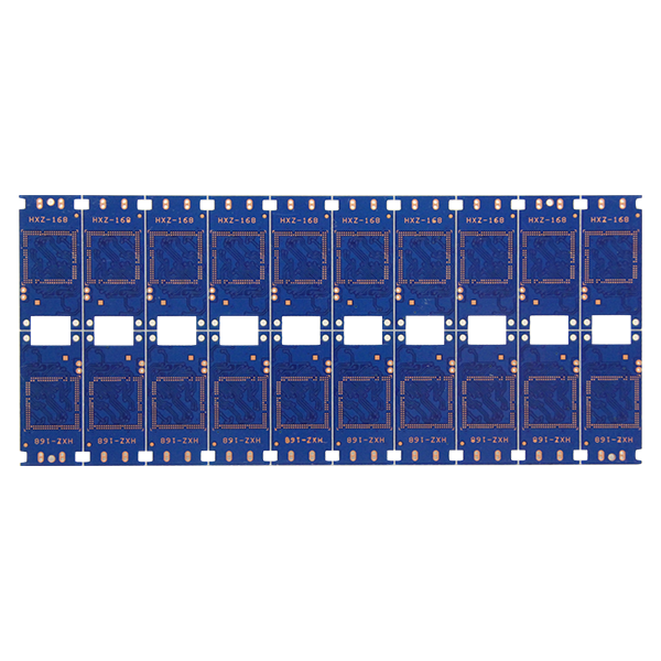
1. The outer frame (clamping edge) of the PCB puzzle should adopt a closed loop design to ensure that the PCB puzzle will be deformed after being fixed on the fixture;
2. PCB puzzle width ≤260mm (SIEMENS line) ≤300mm (FUJI line); if automatic dispensing is required, PCB puzzle width × length≤125 mm × 180 mm;
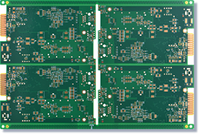
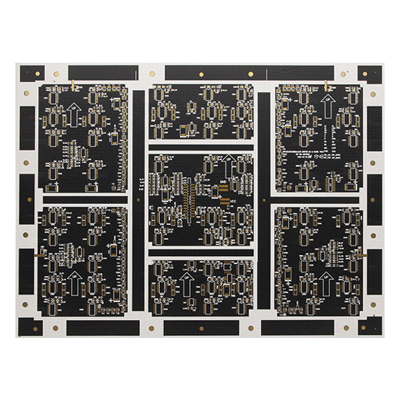
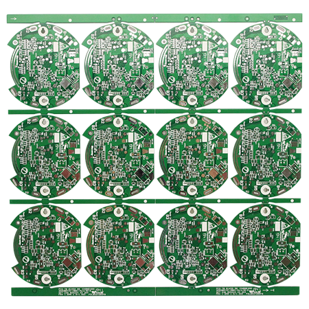
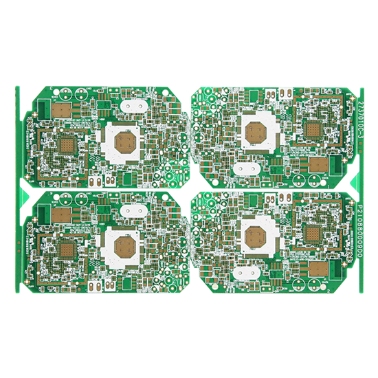
3. The shape of the PCB puzzle is as close to a square as possible. It is recommended to use 2 × 2, 3 × 3,….
4. The center distance between the small plates is controlled between 75 mm 145 mm;

5. When setting the reference positioning point, usually leave a solderless area larger than 1.5 mm around the positioning point;
6. There must be no large devices protruding devices near the connection points between the outer frame of the jigsaw the inner small board, between the small board the small board, the edge of the component the PCB board should leave more than 0.5mm space. To ensure the normal operation of the cutting tool;
7. Four positioning holes are opened at the four corners of the outer frame of the jigsaw, with a hole diameter of 4mm ± 0.01mm; the strength of the hole must be moderate to ensure that it will break during the upper lower plates; the hole position accuracy must be high, the hole wall must be smooth without burrs ;
8. Each small board in the PCB puzzle must have at least three positioning holes, 3 ≤ aperture ≤ 6 mm, wiring patch is allowed within 1 mm of edge positioning holes;
9. The reference symbols used for PCB positioning fine-pitch device positioning. In principle, QFPs with a spacing of less than 0.65mm should be set at their diagonal positions; the positioning reference symbols used for imposition PCB daughter boards should be paired Use, place at the opposite corner of the positioning element;
10.Large components must have positioning posts positioning holes, such as I / O interface, microphone, battery interface, micro switch, headphone interface, motor, etc.
Relevant webpage materials related resources on this site are sourced the Internet. If there is any infringement, please inform us quickly. We will delete it within 24 hours! pcb customization
Telephone:+86-752-3198333
mailbox:sales@xcpcb.net
address:South of Lianfa Avenue, Tongqiao Industrial Park, Zhongkai high tech Zone, Huizhou City, Guangdong Province